Consumables
Highest quality consumables
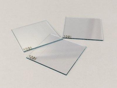
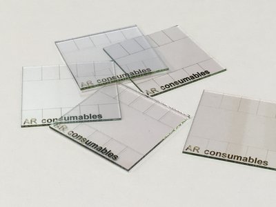
Laser Patterned ITO and FTO Substrates
- High quality substrates for optoelectronic applications, i.e.
- Liquid Crystal Displays (LCD) technology
- Organic Light Emitting Diodes (OLED)
- Organic Photovoltaics (OPV)
- Perovskite Solar Cells
- General Electrochemistry
- Flat Antennas for Mobile Communictaion
- Conducting glass/Transparent electrodes
- Customized pattern
- ITO- or FTO-coated glass
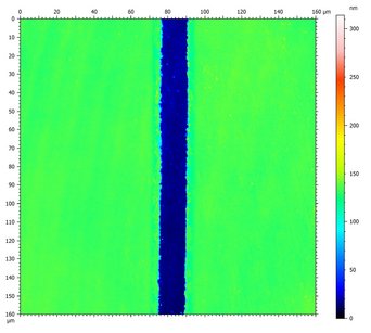
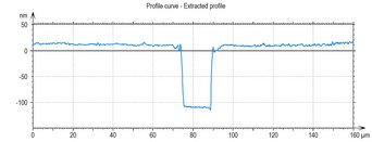
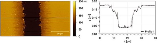
- Laser structured conductive layers with highest precision
- Substrate size up to 200×200 mm²
Transparent, conductive coatings on glass
- Electrical conductivity and optical
transparency - Homogeneously flat ITO/FTO coatings
- Low roughness
- Uniform transmission
General ITO glass properties
- OLED grade, polished, very low roughness,
high transmission - Standard conductivity range 7-20 Ohm/sq
- Glass thickness 0.7-1.1 mm
Laser cut properties
Typically 10-20 μm width, no shunts,
no spikes, no debris
General FTO glass properties
- Low roughness
- Standard conductivity range: 7-13 Ohm/sq
- Glass thickness 1.8-3 mm
- >80% transmission